
Semicon 2.0
- 18 Jul 2026
In News:
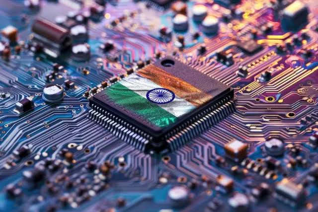
The Union Cabinet has approved Semicon 2.0 with a budgetary outlay of ?1,27,500 crore to accelerate India's semiconductor design and manufacturing ecosystem and strengthen the India Semiconductor Mission (ISM).
About Semicon 2.0
Semicon 2.0 is a long-term policy initiative aimed at developing a complete semiconductor ecosystem in India. Building on the progress achieved under Semicon 1.0, the scheme seeks to strengthen the country's capabilities across the semiconductor value chain—from chip design and fabrication to packaging, research, materials and skilled manpower. The broader objective is to position India as a globally competitive semiconductor hub, reduce import dependence, and enhance technological self-reliance.
Key Features
The scheme adopts a six-pillar approach to build a robust semiconductor ecosystem:
- Design Ecosystem: Promote indigenous semiconductor chip design, intellectual property (IP) and system development, building upon the work of over 105 chip-design startups.
- Machines & Materials:Incentivise manufacturing of semiconductor fabrication equipment, precision machinery, specialty chemicals, materials and gases, thereby strengthening domestic supply chains.
- Semiconductor Fabs: Encourage the establishment of additional silicon fabs, compound semiconductor fabs, discrete component fabs and display fabs. India's first silicon fab is expected to become operational in 2028.
- ATMP/OSAT Facilities: Expand Assembly, Testing, Marking & Packaging (ATMP) and Outsourced Semiconductor Assembly & Test (OSAT) units to make India a preferred destination for advanced semiconductor packaging.
- Research & Development: Promote development of advanced semiconductor nodes, moving beyond the present 28 nm–110 nm technologies through collaboration with leading research institutions.
- Talent Development: Strengthen semiconductor education by expanding training in chip design, clean-room operations, fabrication and ecosystem management, building on the training of 68,000 students across 315 universities.
Progress under Semicon 1.0
Semicon 1.0 has laid the foundation for India's semiconductor ecosystem. So far, 12 manufacturing projects involving an investment of over ?1.64 lakh crore have been approved, including one silicon fab, one silicon carbide fab, one Gallium Nitride (GaN) Micro-LED display fab and nine packaging units. Commercial production has already commenced at Micron, Kaynes and CG Semi.
On the design front, 24 semiconductor design projects have received financial assistance, while 105 startups and MSMEs have been provided access to industry-standard Electronic Design Automation (EDA) tools for developing chips used in sectors such as AI, IoT, drones, satellite communication, telecom and smart devices.