India Semiconductor Mission
- 10 May 2026
In News:
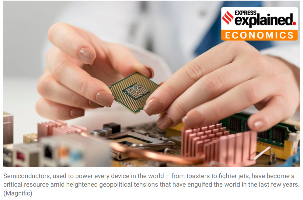
India’s ambition to become a global electronics powerhouse has reached a pivotal juncture. With the recent approval of two major projects in Gujarat—including the nation’s first commercial Gallium Nitride (GaN)-based Mini/Micro-LED display facility and a semiconductor packaging unit—the total number of approved plants under the India Semiconductor Mission (ISM) 1.0 has risen to twelve. These facilities, spread across Gujarat, Assam, Andhra Pradesh, Uttar Pradesh, and Odisha, signal the beginning of a domestic chip revolution.
ISM 1.0: Building the Foundation (2021–2025)
Launched in 2021 under the Ministry of Electronics and Information Technology (MeitY), ISM 1.0 was initiated with a financial outlay of ?76,000 crore. The primary objective was to break India’s near-total dependence on imported chips by incentivizing:
- Semiconductor Fabrication (Fabs): Setting up the complex plants required to print circuits on silicon wafers.
- Display Manufacturing: Reducing reliance on foreign displays for consumer electronics.
- Compound Semiconductors and Packaging: Focusing on Outsourced Semiconductor Assembly and Test (OSAT) and Assembly, Testing, Marking, and Packaging (ATMP) units.
The current trajectory suggests that by 2029, India will possess the capability to design and manufacture chips for 70–75% of domestic applications, with a long-term goal of becoming a top-tier semiconductor nation by 2035.
ISM 2.0: The Shift Toward Indigenous IP and Localisation
Building on the success of the first phase, the Union Budget 2026–27 introduced ISM 2.0. This phase represents a strategic shift from merely attracting global manufacturers to building a "full-stack" indigenous ecosystem.
Key Features of ISM 2.0:
- Strategy and Funding: A broader $11 billion strategy aimed at deepening ecosystem localization.
- Indigenous IP Design: Moving beyond assembly to creating Indian-owned Intellectual Property (IP) and chip designs.
- Supply Chain Fortification: Supporting ancillary industries, including specialty chemicals, gases, and capital goods (manufacturing equipment), which are critical for chip production.
- Materials and Equipment: Reducing the "import intensity" of the manufacturing process itself by encouraging the domestic production of raw materials.
Technological and Strategic Significance
The development of specialized facilities, such as the GaN-based Micro-LED plant, is particularly significant. Gallium Nitride is a "wide-bandgap" semiconductor that is more efficient than traditional silicon, especially for power electronics and advanced displays.
The integration of these twelve plants into the national landscape serves several strategic purposes:
- Supply Chain Resilience: By diversifying manufacturing across five states, India mitigates the risk of localized disruptions and strengthens its position in the global value chain.
- Cross-Sectoral Impact: The chips produced will cater to high-growth sectors, including Automotive (EVs), Telecom (5G/6G), Aerospace, Industrial Automation, and Power.
- Reduced External Dependence: Domestic packaging and testing facilities ensure that even if some wafers are imported, the value addition and final security checks happen on Indian soil.
- Economic Multiplier: The mission fosters a "hub-and-spoke" model where large fabrication units (hubs) attract hundreds of smaller component and material suppliers (spokes).
India Semiconductor Mission
- 20 Aug 2025
In News:
The Union Cabinet has cleared four new semiconductor manufacturing projects worth ?4,600 crore in Odisha, Punjab, and Andhra Pradesh under the India Semiconductor Mission (ISM). With this, the total number of approved projects under ISM has reached ten across six states, attracting cumulative investments of nearly ?1.60 lakh crore.
Details of Newly Approved Units
- SiCSem Pvt. Ltd. (Odisha):
- In partnership with UK-based Clas-SiC Wafer Fab Ltd.
- India’s first commercial compound semiconductor fabrication unit focused on Silicon Carbide (SiC) devices.
- Capacity: 60,000 wafers and 96 million packaged units annually.
- 3D Glass Solutions Inc. (Odisha):
- Will establish a vertically integrated packaging and embedded glass substrate unit.
- Focus: 3D Heterogeneous Integration modules.
- ASIP Technologies (Andhra Pradesh):
- Joint venture with APACT Co. Ltd., South Korea.
- Annual capacity: 96 million units.
- Applications: Mobile phones, set-top boxes, automobiles, and other electronic devices.
- Continental Device India Pvt. Ltd. (Punjab):
- Brownfield expansion of its Mohali facility.
- Focus: High-power discrete devices – MOSFETs, IGBTs, Schottky diodes, and transistors (using both silicon and SiC).
- Capacity: 158.38 million units annually.
Production from these units is expected to commence within the next 2–3 years.
Progress under ISM
- Launch Year: 2021
- Nodal Ministry: Ministry of Electronics and Information Technology (MeitY)
- Objective: Establish a self-reliant semiconductor and display ecosystem in India.
- Support: Incentive package of ?75,000 crore for fabs, ATMP/OSAT, compound semiconductor plants, and display fabs.
- Capacity Building: Target to train 60,000+ skilled professionals.
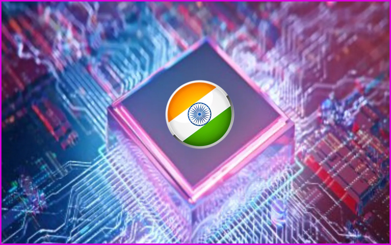
- Strategic Significance: Reduce import dependency, boost Atmanirbhar Bharat, and make India a global semiconductor hub.
Major Ongoing Projects under ISM
- Tata-PSMC Fab (Dholera, Gujarat): ?91,526 crore investment; capacity of 50,000 wafers/month for automotive and AI; operational by 2026.
- Micron ATMP (Sanand, Gujarat): ?22,900 crore investment; focus on DRAM and NAND packaging; expected by late 2025.
- Tata TSAT OSAT (Jagiroad, Assam): Output of 48 million chips/day.
- Kaynes OSAT (Sanand, Gujarat): Capacity of 6 million chips/day for telecom and industrial use.
- HCL–Foxconn JV (Uttar Pradesh): To produce 36 million display driver chips/month by 2027.
India Semiconductor Mission (ISM)
- 04 Sep 2024
In News:
The Union Cabinet, chaired by Prime Minister Narendra Modi, approved the proposal of Kaynes Semicon Pvt Ltd to setup a semiconductor unit in Sanand, Gujarat, with an investment of Rs 3,300 crore.
Key Highlights:
- The proposed unit, under the India Semiconductor Mission (ISM), will produce nearly 60 lakh chips per day.
- The chips produced in this unit will cater to a wide variety of applications which include segments such as industrial, automotive, electric vehicles, consumer electronics, telecom and mobile phones, etc.
- The initiative aligns with India’s goal of developing indigenous semiconductor capabilities.
- As per the reports, India’s semiconductor market is projected to reach $64 billion by 2026, positioning the country as a major global semiconductor hub.
- The first indigenously-developed chip is set to arrive in the country by the end of this year.
- In March, PM Modi laid the foundation stone of three semiconductor projects worth Rs 1.25 lakh crore.
- Tata Electronics is setting up a semiconductor fab in Dholera, Gujarat and one semiconductor unit in Morigaon, Assam.
- CG Power is setting up one semiconductor unit in Sanand. These units will produce lakhs of direct and indirect jobs.
- These four units will bring an investment of almost Rs 1.5 Lakh crore. The cumulative capacity of these units is about 7 crore chips per day, according to the Ministry of Electronics & IT.
- The Programme for Development of Semiconductors and Display Manufacturing Ecosystem in India was notified in 2021 with a total outlay of Rs 76,000 crore.
About India Semiconductor Mission (ISM)
- It is a specialized and independent Business Division within the Digital India Corporation that aims to build a vibrant semiconductor and display ecosystem to enable India’s emergence as a global hub for electronics manufacturing and design.
- ISM has all the administrative and financial powers and is tasked with the responsibility of catalysing the India Semiconductor ecosystem in manufacturing, packaging, and design.
- ISM has an advisory board consisting of some of the leading global experts in the field of semiconductors.
- ISM has been working as a nodal agency for the schemes approved under the Semicon India Programme.
Semicon India Programme:
- Launched in 2021 with a total budget of Rs. 76,000 crore, the ISM is overseen by the Ministry of Electronics and IT (MeitY), Government of India. This initiative is part of a broad effort to develop a sustainable semiconductor and display ecosystem within the country.
- The programme is designed to offer financial support to companies involved in semiconductor and display manufacturing and design. It also aims to foster the creation of domestic Intellectual Property (IP), and to promote and incentivize the Transfer of Technologies (ToT).
- Under this programme, four key schemes have been introduced:
- Scheme for establishing Semiconductor Fabs in India.
- Scheme for establishing Display Fabs in India.
- Scheme for setting up Compound Semiconductors/Silicon Photonics/Sensors Fabs and Semiconductor Assembly, Testing, Marking, and Packaging (ATMP)/OSAT facilities in India.
- Design Linked Incentive (DLI) Scheme.