2D Materials
- 11 Sep 2025
In News:
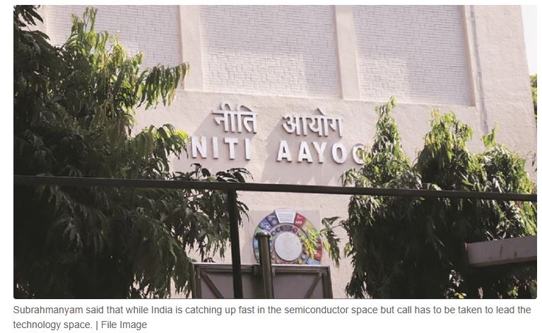
- NITI Aayog’sFrontier Tech Hub, in collaboration with IISc Bengaluru, released the 4th edition of FutureFront Quarterly Insights titled “Introduction to 2D Materials”.
- Report highlights the need for India to invest early in 2D materials to lead in semiconductors, quantum technologies, and advanced electronics.
What are 2D Materials?
- Definition: Materials that are one atom thick, with unique electrical, thermal, and mechanical properties.
- Discovery: Graphene isolated in 2004 → Nobel Prize in Physics, 2010.
- Examples:
- Graphene (Carbon-based)
- Transition Metal Dichalcogenides (TMDCs) –MoS?, WS?
- Hexagonal Boron Nitride (h-BN)
- Xenes – Silicene, Phosphorene
Key Properties
- ~200× stronger than steel, yet flexible.
- Conducts electricity better than copper; spreads heat efficiently.
- Tunable band gaps → useful for semiconductors.
- Exhibits quantum effects (e.g., spin–valley coupling).
- Transparent & flexible → foldable/wearable electronics.
Applications
- Semiconductors: Chips up to 10× smaller than silicon-based chips.
- Quantum Computing: Hosting qubits, spin–valley interactions.
- Artificial Intelligence: Atom-thin memristors for neuromorphic computing.
- Optoelectronics: LEDs, photodetectors, ultra-thin solar cells.
- Green Tech: EV batteries, water filtration, aerospace composites.
Significance for India
- Tech Geopolitics: Control over supply chains and standards creates “tech choke points.”
- Challenge: Current reliance on licensed technologies → dependency (“umbilical cord” risk).
- Opportunity: Early push in 2D materials offers first-mover advantage in semiconductors.
- Global Status: USA, China, Japan, South Korea already investing heavily.
Policy Measures
- NITI Aayog: Urges creation of a complete 2D ecosystem – R&D, talent, supply chains, standards, manufacturing.
- MeitY& DST: Invited proposals for R&D and product development in 2D materials.